📌 UPDATE — March 25, 2026
Ground-level progress is now visible at Giga Texas: site clearing has officially begun on the east side of the property for the new Advanced Technology Fab. Aerial footage captured by drone journalist Joe Tegtmeyer on March 25 shows active clearing work underway, signaling that the project has moved from planning into early construction. The same flyover also revealed the test track on-site taking shape, with distinct features beginning to emerge. This marks a tangible step forward for Tesla's in-house chip manufacturing ambitions discussed in the original article.
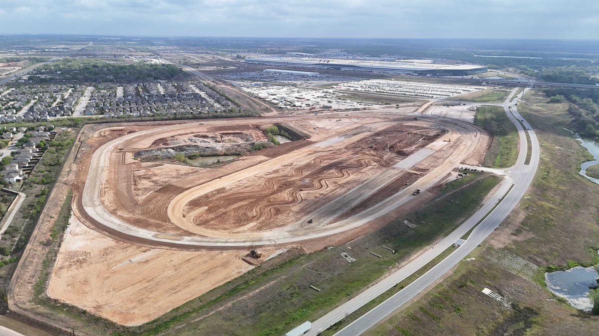
📹 Source: @JoeTegtmeyer via X, March 25, 2026
📌 UPDATE — March 23, 2026
Fresh aerial footage from prolific Giga Texas observer Joe Tegtmeyer confirms that massive construction projects are now visibly underway at the Austin factory, with Tegtmeyer explicitly linking the activity to Tesla's previously announced Terafab production plans. The scale of the build-out suggests the expansion is progressing rapidly. Tegtmeyer also spotted an unidentified new structure on-site, posting a separate aerial image and asking followers to speculate on its purpose — hinting that not all of the construction activity has been publicly explained yet. 🔍

📸 March 23 aerial snapshots confirm Terafab-linked construction is well underway — @JoeTegtmeyer

🔍 A mystery structure spotted at Giga Texas — purpose unknown — @JoeTegtmeyer
📌 UPDATE — March 23, 2026
Elon Musk has now confirmed the staggering scale of the Terafab, stating that 100 million square feet is the right order of magnitude for the combined Tesla/SpaceX facility. To put that in perspective, that's equivalent to roughly 3 New York Central Parks, 15 U.S. Pentagons, or 555 Walmart Supercenters — making it one of the largest manufacturing complexes ever conceived. This figure dramatically underscores just how ambitious Tesla and SpaceX's long-term infrastructure plans are, far beyond what most observers had previously imagined.

30-Second Brief
The News: Elon Musk has clarified that the 'advanced technology fab' at Gigafactory Texas and the 'Terafab' are two distinct facilities with different scopes and purposes.
Why It Matters: Tesla, SpaceX, and xAI are building the most ambitious in-house semiconductor operation in history — and understanding the two-phase structure tells you a lot about the timeline for AI5 chips powering your future Tesla.
Source: @TeslaNewswire on X
Terafab vs. Advanced Technology Fab: Elon Musk Clarifies the Distinction at Giga Texas
Confusion has been swirling online about what exactly is being built at and around Gigafactory Texas. On March 22, Elon Musk stepped in to draw a clear line: the advanced technology fab and the Terafab are not the same thing. They serve different functions, operate at different scales, and sit in different locations. Here's the full picture.

📊 Key Figures
| Metric | Value | Context |
|---|---|---|
| Terafab estimated cost | $20B–$25B | Joint venture: Tesla, SpaceX, xAI |
| Annual compute target | 1 terawatt | At full production capacity |
| Process node target | 2 nanometer | Among most advanced nodes in commercial production |
| Initial wafer starts | 100K/month | Target: 1M/month at scale |
| New building space planned | 5.2M+ sq ft | Added to Giga Texas campus by end of 2026 |
| Output allocation (space) | ~80% | Orbital AI satellites (D3 chips) |
| Output allocation (Earth) | ~20% | FSD, Cybercab, Optimus robots |
| Official launch date | March 21, 2026 | Site preparation already underway |
Two Fabs, Two Very Different Jobs
Think of it as a prototype lab versus a full-scale factory. Musk's clarification draws a sharp distinction between the two facilities:
🔬 Advanced Technology Fab
- Located on the existing Giga Texas campus
- Described by Musk as the 'little' fab
- Purpose: rapid iteration on chip designs
- Think: R&D and validation environment
- Operational sooner — infrastructure already exists
🏭 Terafab
- Located on the North Campus of Giga Texas — a separate, larger site
- $20B–$25B joint venture: Tesla + SpaceX + xAI
- Purpose: full-scale chip production at 2nm
- Think: mass manufacturing at unprecedented scale
- Analysts project initial production no earlier than 2027–2028
According to verified reporting, Musk indicated the Terafab project would 'start off with an advanced technology fab in Austin that would have all of the equipment necessary to make chips of any kind.' In other words, the smaller fab isn't a separate program — it's the beachhead. The advanced technology fab validates designs and processes; the Terafab then manufactures them at terawatt scale.
What the Terafab Will Actually Produce
The Terafab isn't just another chip plant. Its ambition is vertical integration of the entire semiconductor stack — design, lithography, fabrication, memory, advanced packaging, and testing — all under one roof. The two primary chip categories targeted are:
- AI5 inference chips — the next-generation silicon destined for Tesla vehicles and Optimus robots
- D3 chips — custom silicon designed for orbital AI satellites
The output split is striking: approximately 80% of Terafab's compute is earmarked for space-based applications, with just 20% allocated to Earth-side use cases including Full Self-Driving, Cybercab, and Optimus. That ratio will likely be a talking point for Tesla investors who want to understand how much chip capacity is actually flowing into the vehicles they own.
🔭 The BASENOR Take
Timeline
2026 (fab) → 2027–28 (Terafab)
Impact Level
🔴 High — Long-term chip supply for all Tesla products
Confidence
⬛⬛⬛⬜ — Launch confirmed, production timeline speculative
Musk's clarification matters because it reframes the narrative. This isn't a single moonshot — it's a staged buildout. The advanced technology fab is the proof-of-concept phase: a relatively nimble facility where Tesla's chip teams can iterate quickly without the overhead of a full-scale foundry. Once designs are locked, the Terafab takes over at a scale that would rival the world's largest semiconductor plants.
For Tesla owners, the 20% Earth-side compute allocation is the number to watch. At 1 terawatt of annual output and 100,000 wafer starts per month scaling to 1 million, even a 20% slice represents an enormous volume of AI5 chips. That's the supply pipeline for the next generation of FSD hardware, Cybercab's autonomous stack, and Optimus. If Terafab hits its targets, Tesla's dependency on third-party chip suppliers — a persistent vulnerability — effectively ends.
The catch is timing. Site preparation is underway north of the existing Giga Texas facility, with permit documents showing plans to add over 5.2 million square feet of new building space by end of 2026. But construction of a 2nm fab is among the most complex engineering challenges in existence. Analysts are right to flag 2027–2028 as a realistic window for initial production. Between now and then, the advanced technology fab on the main campus is where the real chip development action will happen — and that's the facility Musk was pointing to when he said 'little.'
📰 Deep Dive
The timing of Musk's clarification — just one day after the official Terafab launch on March 21 — suggests the two facilities were being conflated in public discourse almost immediately. That's understandable: both involve chip fabrication, both are tied to the Giga Texas geography, and both were announced in close succession. But conflating them leads to a distorted sense of what's operational now versus what's years away.
The joint venture structure of the Terafab is also worth examining. Tesla, SpaceX, and xAI pooling resources for a $20–25 billion semiconductor facility reflects a shared constraint: all three companies need cutting-edge compute at volumes that the open market cannot reliably supply. By building their own foundry, Musk's companies are essentially exiting the global chip allocation queue. The 80/20 split between space and Earth applications tells you which company is the primary driver of demand — but Tesla still benefits enormously from the 20% slice, especially as FSD and Cybercab scale.
What remains to be seen is how the advanced technology fab feeds designs into the Terafab pipeline. If the smaller facility can validate 2nm process designs efficiently, it compresses the timeline for Terafab to reach meaningful production volumes. That's the strategic logic: don't wait for the mega-factory to be ready before you start learning. Run the experiments now, in the 'little' fab on the existing campus, so that when Terafab's lithography machines come online, the chip designs are already proven.
For anyone tracking Tesla's long-term competitive position, this two-fab structure is one of the most consequential infrastructure decisions the company has made. Vertical integration of chips — following the playbook Tesla already ran with battery cells, motors, and software — removes a critical external dependency and gives Tesla direct control over the silicon that will define its vehicles for the next decade.

Sarah focuses on Tesla Energy, SpaceX missions, and the broader Musk AI portfolio. Former data analyst in clean energy. Based in San Francisco.
Sources verified at publish time. Spotted an inaccuracy? Email editorial@basenor.com.