
30-Second Brief
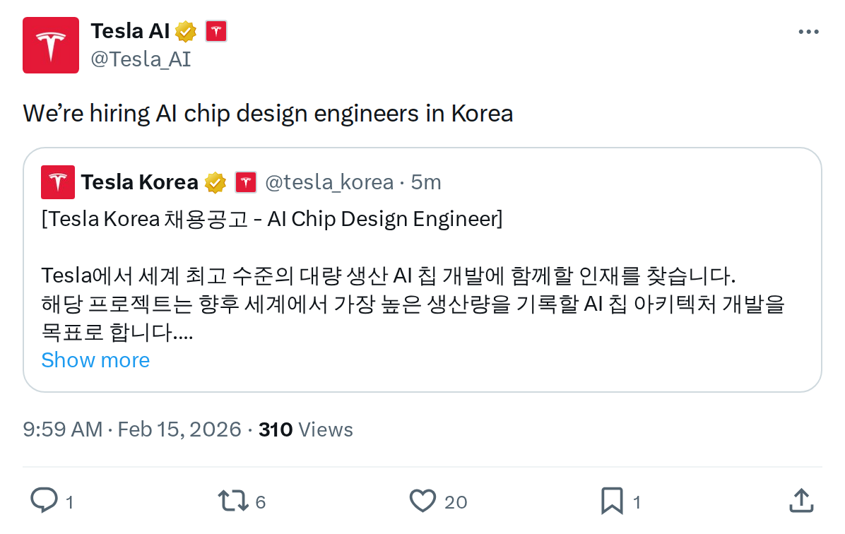
The News: Tesla's AI division announced recruitment for chip design engineers in South Korea, marking a strategic expansion into one of the world's premier semiconductor talent markets.
Why It Matters: This hiring push strengthens Tesla's in-house silicon capabilities for FSD and autonomous systems, directly supporting the development of AI5, AI6, and future chips manufactured through Tesla's $16.5B partnership with Samsung Electronics.
Source: @Tesla_AI on X
Tesla Taps South Korea's Semiconductor Expertise
Tesla's AI division made a direct recruitment appeal early Saturday morning, announcing open positions for chip design engineers in South Korea. The announcement, posted by the official @Tesla_AI account, signals an aggressive expansion of the company's hardware engineering footprint in Asia.

The timing is strategic. South Korea is home to Samsung Electronics, Tesla's primary manufacturing partner for next-generation AI chips, and hosts one of the world's deepest pools of semiconductor engineering talent. According to verified reports, Tesla has already established operations in Hwaseong, Gyeonggi Province — the exact location of Samsung's major wafer fabrication facilities.
📊 Key Figures
| Metric | Value | Context |
|---|---|---|
| Samsung Partnership Value | $16.5 billion | 8-year manufacturing contract through December 2033 |
| Chip Manufacturing Process | 2-nanometer | Samsung's most advanced node for AI5, AI6, AI16 chips |
| Design Cycle Target | 9 months | Reduction from 3-year cycle, per Musk's January 2026 statement |
| Texas Facility Production Start | 2027 | Samsung's Taylor, TX fab expected to ship AI6 chips |
🔭 The BASENOR Take
Timeline: Immediate hiring push, with chips from this team likely influencing AI7+ generations (2028 and beyond)
Impact Level: High — Directly accelerates Tesla's vertical integration in AI silicon development
Confidence: 95% — Confirmed by official Tesla AI account and aligns with verified Samsung partnership details
This recruitment drive represents more than geographic expansion — it's a calculated move to accelerate Tesla's chip design velocity. Elon Musk stated in January 2026 that the AI5 chip design is nearly complete, while AI6 has entered early design stages. The goal: compress the traditional three-year design cycle to just nine months for future iterations through AI9.
By embedding engineers directly in South Korea's semiconductor ecosystem, Tesla gains three strategic advantages:
- Co-location with Manufacturing: Engineers working near Samsung's Hwaseong fab can iterate on designs with faster feedback loops from the production floor.
- Talent Density: South Korea produces world-class chip designers, many with experience at Samsung, SK Hynix, and other tier-one semiconductor companies.
- Time Zone Coverage: A Korea-based team provides around-the-clock development cycles when paired with Tesla's California and Texas engineering groups.
What This Means for Tesla Owners
For current Tesla owners, this hiring push won't change your FSD experience next week — but it's a strong signal about the trajectory of autonomous capabilities over the next 2-3 years.
The AI chips being designed today will power:
- More efficient FSD processing: Next-gen silicon should deliver higher inference speeds with lower power consumption
- Advanced vision systems: Improved neural network architectures for better object detection and path planning
- Future autonomy features: Hardware foundation for unsupervised FSD and potential robotaxi deployment
According to verified reports, Tesla's AI5 chips are expected to be manufactured at Samsung's Hwaseong facility, while AI6 production is slated for Samsung's new Taylor, Texas fab beginning in 2027. The chips designed by this expanded Korea team will likely influence the AI7 generation and beyond.
The Bigger Picture: Vertical Integration
Tesla's approach contrasts sharply with traditional automakers who rely on third-party chip suppliers like NVIDIA or Qualcomm. By designing custom silicon in-house, Tesla can optimize every aspect of the hardware-software stack specifically for vision-based autonomy.
The $16.5 billion Samsung partnership provides the manufacturing muscle, but the intellectual property — the chip architectures, neural network accelerators, and vision processing pipelines — comes from Tesla's own engineers. This Korea hiring push expands that internal capability.
The nine-month design cycle target is particularly ambitious. For context, industry-standard chip development timelines typically span 2-3 years from architecture definition to production-ready silicon. If Tesla achieves this compression, it would enable rapid iteration on AI hardware to match the pace of FSD software updates.
📰 Deep Dive
The semiconductor industry has long operated on Moore's Law time scales — incremental improvements every 18-24 months. Tesla's stated ambition to iterate on chip designs every nine months represents a fundamentally different operational tempo, one borrowed more from software development than traditional hardware engineering.
This is only possible with two conditions: massive capital investment (the $16.5B Samsung deal provides that) and deep engineering talent (which this Korea recruitment aims to secure). South Korea offers both proximity to cutting-edge fabrication facilities and a workforce trained in advanced process nodes. Many Korean chip engineers have spent careers optimizing designs for 5nm, 3nm, and now 2nm manufacturing processes — exactly the expertise Tesla needs for AI5 and AI6 production.
The location choice also reveals Tesla's pragmatic approach to global talent. Rather than requiring all chip designers to relocate to California or Texas, Tesla is building capability where the expertise already exists. This mirrors strategies used by companies like Apple and Google, who maintain semiconductor design centers in multiple countries to access specialized talent pools.
For Tesla owners watching the FSD development roadmap, this hardware investment is the foundation layer. Software improvements grab headlines with each new version release, but the underlying compute architecture determines the ceiling of what's possible. Faster inference engines enable more complex neural networks. More efficient power delivery extends the range impact of running FSD. Better thermal management allows sustained performance during long highway drives. These hardware characteristics are baked into the silicon — and teams like the one Tesla is building in Korea are the ones defining those specifications.

Sarah focuses on Tesla Energy, SpaceX missions, and the broader Musk AI portfolio. Former data analyst in clean energy. Based in San Francisco.
Sources verified at publish time. Spotted an inaccuracy? Email editorial@basenor.com.